Industry insight: photonics to scale AI data centers
By Luis Torrijos-Morán & Daniel Pérez-López
npj Nanophotonics volume 3, Article number: 8 (2026)
Article source:https://www.nature.com/articles/s44310-025-00105-1?utm_source=chatgpt.com
The rapid evolution of artificial intelligence (AI) and its high-performance demands on computational systems have significantly impacted modern data center infrastructure. Conventional scaling strategies are approaching physical and economic limits, necessitating innovations in system-level design and networking technologies. Photonics has emerged as a transformative solution, offering unparalleled bandwidth, energy efficiency, and scalability across multiple layers of data center architecture. This paper explores the adoption of photonic technologies, including co-packaged optics (CPO), optical circuit switches (OCS), and silicon photonics in general, to address critical challenges in interconnect bandwidth, latency, and power consumption. By analyzing their integration at the package, rack, and network levels, we highlight how photonics can overcome the limitations of traditional electronic solutions, paving the way for the next generation of AI infrastructure.
Introduction
The rapid proliferation of transformer-based architectures has driven an unprecedented escalation in AI model complexity, with parameter counts increasing by nearly 200× every two years. To sustain these expanding computational demands, processors such as graphics and tensor processing units (GPUs, TPUs, XPUs) and other specialized accelerators have undergone decades of continuous miniaturization, yielding remarkable improvements in cost efficiency, power consumption, and compute density. However, after more than six decades of exponential scaling, further miniaturization is nearing both physical and economic limits. While advances in chip and system-on-chip (SoC) design will undoubtedly continue, the interconnection of multiple XPUs has become increasingly vital to maintaining system-level performance growth1.
One promising direction is system-in-package (SiP) scaling, which integrates multiple processing units within a single subassembly. Yet, like individual chips, these packages face constraints in area, thermal management, and overall design complexity. Although incremental gains in packaging technology are expected, they alone are insufficient to sustain exponential performance growth, necessitating additional scaling strategies. Consequently, the industry has turned to rack-scale integration, combining multiple SiPs into unified high-performance computing platforms. This trend extends outward across successive layers of integration—packages to racks, racks to clusters, and clusters to full-scale data centers, forming a hierarchically scalable compute infrastructure. As computation scales beyond the chip boundary, networking becomes the foundational enabler of system performance. Each level of this hierarchy introduces greater physical separation and communication complexity, demanding distinct interconnect technologies optimized for the latency, bandwidth, and energy characteristics of their respective layers2.
However, despite continuous improvements in network bandwidth, further growth is facing scalability challenges. Power availability, at both cabinet and data center scales, has emerged as a critical constraint. Networking alone accounts for nearly 10% of total compute power consumption, and this fraction continues to rise with increasing data rates. Reliability presents another major limitation. Large-scale AI clusters comprising hundreds of thousands of transceivers experience frequent component failures, where disruptions in systems of 500,000 XPUs can lead to losses exceeding $3 million per day3.
This paper explores how photonic technologies can address these system-level scaling challenges across the multiple layers of the AI data center—from chip packages to rack-scale and inter-data center networks. We analyze the readiness, potential, and adoption trends of photonic interconnects in redefining the next generation of scalable AI infrastructure.
Scaling challenges and opportunities
Scaling up packages
The most cost-efficient way to interconnect multiple chips within a single package is through electronic traces, which allow for high-speed communication over short distances. A well-known example is the compute-to-memory link provided by HBM3, which delivers approximately 36 TBps of bandwidth over a reach of just 5 mm.
As chip architectures grow more complex and larger, and as their data throughput demands increase, there is growing interest in transitioning to optical interconnects. Two main approaches are being explored to enable this evolution: optical interposers and optical I/O subassemblies.
Optical interposers, as shown in Fig. 1a, are designed to interconnect several XPUs on top of a large optoelectronic carrier, enabling electro-optic communication between cores. This method is currently being developed by companies such as Lightmatter (micro-ring modulators), Lightelligence, and Celestial AI (Electro-absorption Modulators).
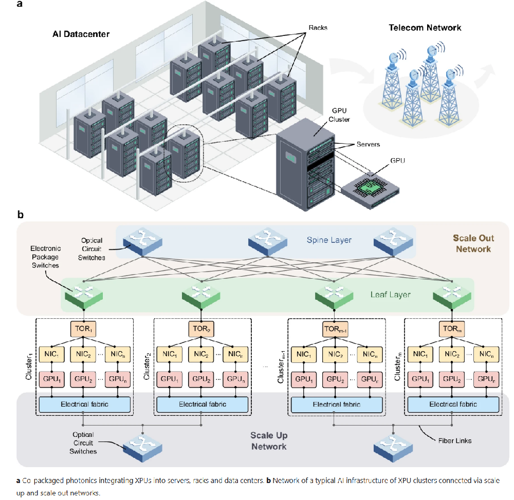
AI data center architecture.
The alternative text for this image may have been generated using AI.a Co-packaged photonics integrating XPUs into servers, racks and data centers. b Network of a typical AI infrastructure of XPU clusters connected via scale up and scale out networks.
In contrast, the optical I/O subassembly approach involves introducing electro-optical interfaces that convert electrical signals into optical ones directly at the chip’s facet. Instead of relying on an optical substrate, this method uses optical fiber as the transmission medium to route signals between different cores or subassemblies within the package. Companies like Samtec and Ayar Labs are actively advancing this technology.
Scaling up racks
Standalone servers with a limited number of XPUs are no longer sufficient to compute and manage the massive number of parameters required by today’s advanced AI models. Figure 1a illustrates a conventional data center architecture in which XPUs are organized into racks, forming compute clusters or “islands”. Within each cluster, XPUs are interconnected through a scale-up network using high-bandwidth electrical fabrics such as Nvidia’s NVLink or AMD’s Infinity Interconnect, as shown in Fig. 1b. This part of the network is optimized for efficient communication and is primarily used to transfer large volumes of data between XPUs.
However, the limited reach of traditional copper interconnects in the scale-up network imposes a cap on the number of XPUs that can be included in a single cluster—typically between 72 and 144 units. This limitation restricts the degree of XPU data parallelism, leading to longer training times for large AI models.
To address these constraints and extend the scale-up network at the rack level, two main solutions are emerging. One approach focuses on co-packaged optics, aiming to integrate electronic switching within the rack while using fiber links for interconnection—Broadcom is an example of a company advancing this technology. An alternative approach leverages silicon photonic optical circuit switches (OCS) in combination with optical I/O solutions3. These enable sub-millisecond reconfiguration times and ultra-low port-to-port latency. Companies such as iPronics and nEye are actively developing fast-reconfigurable OCS technologies to support this next-generation network architecture.
Scaling up data centers
Beyond the compute island, connectivity is achieved through multiple tiers of switches that form the scale-out network. These switches, typically electronic packaged switches (EPS), are organized into configurations such as fat-tree networks or other topologies. Compared to the scale-up network, the scale-out network offers more limited bandwidth, resulting in less efficient data communication. Consequently, AI model parallelism strategies must be meticulously designed to maximize performance within these network constraints. The stagnation in electronics innovation, particularly in clock speed, further impedes the development of faster switches with higher aggregate bandwidth. Moreover, the diminishing efficiency of electrical processors demands substantial power, and the energy required to transfer large volumes of data further exacerbates this issue, compromising overall energy efficiency. To mitigate this, companies like Nvidia or Broadcom have presented CPO switches both for ethernet and InfiniBand with the benefits of networking for massive-scale infrastructure with reduced power consumption, high resiliency, faster deployment and reduced latency.
Similarly, high-radix OCS based on Micro-Electro-Mechanical Systems (MEMS) and Liquid Crystal on Silicon (LCOS) technologies are garnering significant attention for deployment within the Spine layer of modern networks. Pioneer companies like Google have integrated OCS into their AI infrastructure to enhance reliability and enable higher-bandwidth communication between compute islands4. Other notable companies investing in OCS for AI networks include Lumentum, Coherent, Polatis (H&S) and iPronics.
Industry landscape and adoption
The deployment of photonic technologies across data center hierarchies is progressing unevenly. Some domains, such as pluggable transceivers, are fully mature and commercially ubiquitous, while others, like co-packaged optics and optical circuit switches, exhibit high technical readiness but are on early-adoption phase. Table 1 summarizes the main technologies and their current levels of adoption representing both technical maturity and adoption readiness.
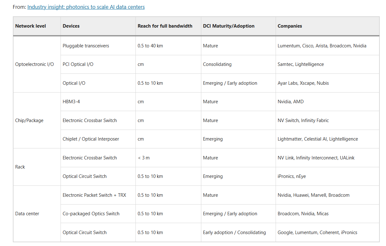
Table 1 Some photonic and electronic networking technologies across data center hierarchy showing approximate maturity and adoption readiness levels
For most of these technologies, cost-effectiveness remains the primary barrier to widespread adoption of optical solutions. Nevertheless, photonics is not merely replacing electrical interconnects but reshaping data center architectures and enabling new opportunities for performance and reliability enhancement. One notable example is the use of optical circuit switches (OCS) in scale-out networks, which can eliminate the traditional spine layer and enable bandwidth engineering to mitigate traffic congestion5. Photonic interconnects can also extend scale-up networks beyond hundreds of XPUs, enhancing data parallelism and supporting direct connectivity between compute islands. Communication latency is significantly reduced since data remains in the optical domain and switching occurs at the physical layer, avoiding signal conversions, buffering, and other delays typical of electronic packet switches (EPS) with pluggable transceivers. Moreover, optical fabrics inherently improve resiliency6, supporting programmable recovery and autonomous fault mitigation at the physical layer, thereby lowering operational costs and improving reliability. Finally, optical fabrics enable dynamic topology reconfiguration, creating locally adaptive, high-bandwidth domains that greatly benefit distributed training, particularly in mixture-of-experts (MoE) and other communication-intensive AI workloads
The path forward: Open questions for Nanophotonics
The next phase of AI data center evolution will be driven by the convergence of system-level architectural innovation and advances in integrated photonics hardware. Over the coming years, research and development must progress along two complementary fronts: (1) programmable network architectures that leverage optical reconfigurability, and (2) hardware breakthroughs that enhance modulation speed, switch scalability, and packaging efficiency.
A. System-Level Architectures and Software Advances
Emerging optical fabrics are increasingly being designed to adapt to dynamic traffic patterns, enabling more efficient and scalable data movement across large AI clusters. Two main paradigms are shaping this evolution: traffic-aware (TA) architectures—exemplified by Jupiter, Helios, Mordia, and more recently Vermilion—and traffic-oblivious (TO) architectures such as RotorNet and Opera9,10.
TA systems rely on real-time telemetry and network control to allocate optical bandwidth where it is most needed, dynamically reconfiguring topologies in response to workload demands. In contrast, TO systems employ deterministic or periodic switching schedules that provide predictable performance with minimal control overhead. Increasingly, research is exploring hybrid optical fabrics that combine the predictability of TO networks with the flexibility of TA reconfiguration to optimize performance under bursty or evolving traffic conditions.
Future work will extend these paradigms beyond inter-rack networking toward rack-scale and package-level optical switching, enabling optical “scale-up” communication within tightly coupled accelerator domains. Achieving this vision will require standardization across network control software11, photonic switching hardware, and distributed AI training frameworks to fully exploit the potential of dynamic optical topologies for large-scale computing.
B. Hardware Advances in Integrated Optics
Progress in integrated photonics remains fundamental to unlocking the scalability and efficiency of next-generation AI data centers.
On the co-packaged optics (CPO) front, four directions of improvement are particularly relevant: (i) tighter integration with CMOS electronics to achieve cost-effective high-speed transmission; (ii) increased bandwidth density at the optical faceplate; (iii) further reductions in power consumption compared to retimed electrical optics; and (iv) enhanced system reliability to meet data center deployment requirements.
In optical switching, research is focusing on low-loss, large-radix integrated designs capable of achieving insertion losses below 2–3 dB, fiber-to-chip coupling losses below 0.5 dB per facet, and scalable optical circuit switches exceeding 64–128 ports in a cost-efficient form factor. These developments aim to reduce network power consumption, minimize latency, and enable sub-millisecond reconfiguration times suited to workload-adaptive AI fabrics.
For optical I/O, advances in materials such as thin-film lithium niobate (LiNbO₃), barium titanate (BTO), and plasmonic silicon are driving a new generation of high-speed, low-power modulators with bandwidths exceeding 100 GHz, sub-pJ/bit energy efficiencies, and improved thermal stability. Combined with next-generation CPO architectures, these devices will deliver unprecedented bandwidth and energy efficiency directly at the compute package level both for single and multiple wavelength transceivers.
At the chip-to-chip interconnect level, the growing bandwidth demands of multi-chip modules (MCMs) are exposing the limitations of electrical die-to-die communication in both bandwidth density and energy overhead. Silicon-based optical interposers offer a promising path to alleviate these constraints by increasing beachfront and area bandwidth density. Although challenges remain regarding interposer size, thermal management, and co-design with electronics chips, active research investment is rapidly advancing the scalability and manufacturability of these platforms.
C. Outlook
As photonic hardware and adaptive network control continue to mature in unison, AI data centers will evolve into programmable optical systems capable of reshaping their topology dynamically in response to workload demands. These advances promise substantial gains in bandwidth density, latency reduction, and energy efficiency, while maintaining the flexibility required by modern AI training frameworks. The close integration of intelligent control software with scalable photonic interconnects will ultimately define the foundation of next-generation AI infrastructure—where light becomes not merely the medium of communication, but the driving enabler of compute scalability itself.
Conclusions
This work has examined the growing role of photonics in addressing the limitations of traditional electronic interconnects within modern data centers. From co-packaged optics at the board level to silicon photonics and optical circuit switches at the rack and network levels, photonics enables significant advances in bandwidth, energy efficiency, latency, and system scalability. These technologies not only alleviate bottlenecks in the network but also provide flexible, resilient, and high-performance solutions for the evolving demands of AI-driven applications. As models and computational requirements continue to scale, the integration of photonics will play a pivotal role in shaping future data center architectures, driving innovation in AI capabilities and laying the groundwork for a more efficient, reliable, and sustainable future.
References
D. O’Laughlin, “The Data Center is the New Compute Unit: Nvidia’s Vision for System-Level Scaling”, fabricatedknowledge.com (2024)
Sato, K.-i. Optical switching will innovate intra data center networks [Invited Tutorial]. J. Optical Commun. Netw. 16, A1–A23 (2023).
NVIDIA. “Keynote at ECOC 2025.” ECOC Keynote Speech (2025).
Khani, M. et al. “SiP-ML: high-bandwidth optical network interconnects for machine learning training.” Proceedings of the 2021 ACM SIGCOMM 2021 Conference. 2021.
Poutievski, L. et al. “Jupiter evolving: transforming google’s datacenter network via optical circuit switches and software-defined networking.” Proceedings of the ACM SIGCOMM 2022 Conference. 2022.
Sato, K.-i. Realization and application of large-scale fast optical circuit switch for data center networking. J. Lightwave Technol. 36, 1411–1419 (2018).
Patronas, G. et al. Optical switching for data centers and advanced computing systems [Invited]. J. Opt. Commun. Netw. 17, A87–A95 (2025).
Liao, X. et al. mFabric: An Efficient and Scalable Fabric for Mixture-of-Experts Training. arXiv preprint arXiv:2501.03905 (2025).
Addanki, V. et al. “Vermilion: A Traffic-Aware Reconfigurable Optical Interconnect with Formal Throughput Guarantees.” arXiv preprint arXiv:2504.09892 (2025).
Farrington, N. et al. “Helios: a hybrid electrical/optical switch architecture for modular data centers.” Proceedings of the ACM SIGCOMM 2010 Conference. 2010.
Open Compute Project. “Optical Circuit Switching.” Open Compute Project, 2025, https://www.opencompute.org/projects/optical-circuit-switching.

SUZHOU InnovSemi CO.,LTD